SR latch: Difference between revisions
(Created page with "thumb|Figure 1. SR latch circuit and truth table The '''set-reset latch''' is a circuit that stores a value in a bistable circuit using two NOR gates. It is the fundamental building block for memory cells.") |
No edit summary |
||
| (2 intermediate revisions by the same user not shown) | |||
| Line 1: | Line 1: | ||
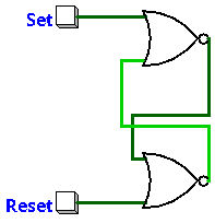
[[File:SR | [[File:SR latch schematic.png|thumb|Figure 1. Schematic of an SR latch]] | ||
The '''set-reset latch''' is a circuit that stores a value in a [[bistable]] circuit using two NOR gates. It is the fundamental building block for memory cells. | The '''set-reset latch''' is a circuit that stores a value in a [[bistable]] circuit using two NOR gates. It is the fundamental building block for memory cells. | ||
= Behavior = | |||
As pictured in Figure 1, it ''latches'' a bit value when the input is 0,0, saving it (and its complement) in the outputs of the NOR gates. | |||
Pressing ''Set'' (1,0) or ''Reset'' (0,1)will change the value of the saved bit accordingly | |||
If both ''Set'' and ''Reset'' are input (1,1), the circuit oscillates. | |||
= Principle = | |||
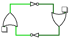
The simplest form of storing a bit value is two NOT gate linked together. This will store a ''HIGH'' and a ''LOW'' in a loop. | |||
[[File:SR latch with not.png|thumb|Figure 2. NOT loop saves a value, while OR gates send pulses into the circuit]] | |||
By sending a ''HIGH'' pulse to the previous ''LOW'', we can swap them. The pulse is sent by an OR gate. The circuit is shown in Figure 2. This is trivially equivalent to the circuit shown in Figure 1. | |||
An enabler can be integrated with AND gates. By fluctuating the enabler at set time intervals, we get a '''clocked D-latch'''. | |||
Note that it is an ''abstraction'' and may be [[astable]] | |||
The D-latch acts on level. This messes up the clock cycle. | |||
[[Category:Computer Architecture]] | |||
Latest revision as of 20:23, 6 May 2024

The set-reset latch is a circuit that stores a value in a bistable circuit using two NOR gates. It is the fundamental building block for memory cells.
Behavior
As pictured in Figure 1, it latches a bit value when the input is 0,0, saving it (and its complement) in the outputs of the NOR gates.
Pressing Set (1,0) or Reset (0,1)will change the value of the saved bit accordingly
If both Set and Reset are input (1,1), the circuit oscillates.
Principle
The simplest form of storing a bit value is two NOT gate linked together. This will store a HIGH and a LOW in a loop.

By sending a HIGH pulse to the previous LOW, we can swap them. The pulse is sent by an OR gate. The circuit is shown in Figure 2. This is trivially equivalent to the circuit shown in Figure 1.
An enabler can be integrated with AND gates. By fluctuating the enabler at set time intervals, we get a clocked D-latch.
Note that it is an abstraction and may be astable
The D-latch acts on level. This messes up the clock cycle.
